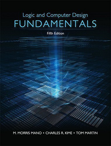
Logic and Computer Design Fundamentals 5th Edition by M. Morris Mano, ISBN-13: 978-0133760637
Original price was: $50.00.$14.99Current price is: $14.99.
Safe & secure checkout
Description
Description
Trustpilot
Logic and Computer Design Fundamentals 5th Edition by M. Morris Mano, ISBN-13: 978-0133760637
[PDF eBook eTextbook] – Available Instantly
- Publisher: Pearson; 5th edition (March 4, 2015)
- Language: English
- 672 pages
- ISBN-10: 0133760634
- ISBN-13: 978-0133760637
For courses in Logic and Computer design.
Understanding Logic and Computer Design for All Audiences.
Logic and Computer Design Fundamentals is a thoroughly up-to-date text that makes logic design, digital system design, and computer design available to readers of all levels. The Fifth Edition brings this widely recognized source to modern standards by ensuring that all information is relevant and contemporary. The material focuses on industry trends and successfully bridges the gap between the much higher levels of abstraction people in the field must work with today than in the past.
Broadly covering logic and computer design, Logic and Computer Design Fundamentals is a flexibly organized source material that allows instructors to tailor its use to a wide range of audiences.
Table of Contents:
Contents
Preface
New to This Edition
Logic and Computer Design Fundamentals
CHAPTER 1 Digital Systems and Information
1-1 Information Representation
The Digital Computer
Beyond the Computer
More on the Generic Computer
1-2 Abstraction Layers in Computer Systems Design
An Overview of the Digital Design Process
1-3 Number Systems
Binary Numbers
Octal and Hexadecimal Numbers
Number Ranges
1-4 Arithmetic Operations
Conversion from Decimal to Other Bases
1-5 Decimal Codes
1-6 Alphanumeric Codes
ASCII Character Code
Parity Bit
1-7 Gray Codes
1-8 Chapter Summary
References
Problems
CHAPTER 2 Combinational Logic Circuits
2-1 Binary Logic and Gates
Binary Logic
Logic Gates
HDL Representations of Gates
2-2 Boolean Algebra
Basic Identities of Boolean Algebra
Algebraic Manipulation
Complement of a Function
2-3 Standard Forms
Minterms and Maxterms
Sum of Products
Product of Sums
2-4 Two-Level Circuit Optimization
Cost Criteria
Map Structures
Two-Variable Maps
Three-Variable Maps
2-5 Map Manipulation
Essential Prime Implicants
Nonessential Prime Implicants
Product-of-Sums Optimization
Don’t-Care Conditions
More Optimization
2-6 Exclusive-or Operator and Gates
Odd Function
2-7 Gate Propagation Delay
2-8 HDLs Overview
Logic Synthesis
2-9 HDL Representations—VHDL
2-10 HDL Representations—Verilog
2-11 Chapter Summary
References
Problems
CHAPTER 3 Combinational Logic Design
3-1 Beginning Hierarchical Design
Specification:
Formulation:
Optimization:
3-2 Technology Mapping
3-3 Combinational Functional Blocks
3-4 Rudimentary Logic Functions
Value-Fixing, Transferring, and Inverting
Multiple-Bit Functions
The Problem:
The Solution:
Enabling
The Problem:
The Solution:
3-5 Decoding
Decoder and Enabling Combinations
Decoder-Based Combinational Circuits
3-6 Encoding
Priority Encoder
Encoder Expansion
3-7 Selecting
Multiplexers
The Problem:
The Solution:
Multiplexer-Based Combinational Circuits
Specification:
Formulation:
Optimization:
3-8 Iterative Combinational Circuits
3-9 Binary Adders
Half Adder
Full Adder
Binary Ripple Carry Adder
3-10 Binary Subtraction
Complements
Subtraction Using 2s Complement
3-11 Binary Adder-Subtractors
Signed Binary Numbers
Signed Binary Addition and Subtraction
The Problem:
The Solution:
Overflow
MULTIPLIERS AND DIVIDERS
HDL Models of Adders
Behavioral Description
3-12 Other Arithmetic Functions
Contraction
Incrementing
Decrementing
Multiplication by Constants
Division by Constants
Zero Fill and Extension
Decimal Arithmetic
3-13 Chapter Summary
References
Problems
CHAPTER 4 Sequential Circuits
4-1 Sequential Circuit Definitions
4-2 Latches
SR and S─ R─ Latches
D Latch
4-3 Flip-Flops
Edge-Triggered Flip-Flop
Standard Graphics Symbols
Direct Inputs
Flip-Flop Timing
4-4 Sequential Circuit Analysis
Input Equations
State Table
State Diagram
SEQUENTIAL CIRCUIT CLOCKS AND TIMING
Sequential Circuit Simulation
4-5 Sequential Circuit Design
Design Procedure
Finding State Diagrams and State Tables
State Assignment
Designing with D Flip-Flops
Designing with Unused States
Verification
4-6 State-Machine Diagrams and Applications
State-Machine Diagram Model
Constraints on Input Conditions
Design Applications Using State-Machine Diagrams
Asynchronous Interfaces, Synchronization, and Synchronous Circuit Pitfalls
4-7 HDL Representation for Sequential Circuits—VHDL
4-8 HDL Representation for Sequential Circuits—Verilog
4-9 Flip-Flop Timing
4-10 Sequential Circuit Timing
4-11 Asynchronous Interactions
4-12 Synchronization and Metastability
4-13 Synchronous Circuit Pitfalls
4-14 Chapter Summary
References
Problems
CHAPTER 5 Digital Hardware Implementation
5-1 The Design Space
Integrated Circuits
Levels of Integration
CMOS Circuit Technology
CMOS Transistor
CMOS Transistor Models
Circuits of Switches
Fully Complementary CMOS Circuits
Technology Parameters
FAN-IN
Fan-Out
Cost
5-2 Programmable Implementation Technologies
Read-Only Memory
Programmable Logic Array
Combinational Circuit Implementation Using a PLA
Programmable Array Logic Devices
Combinational Circuit Implementation with a PAL Device
Field Programmable Gate Array
5-3 Chapter Summary
References
Problems
CHAPTER 6 Registers and Register Transfers
6-1 Registers and Load Enable
Register with Parallel Load
6-2 Register Transfers
6-3 Register Transfer Operations
6-4 Register Transfers in VHDL and Verilog
6-5 Microoperations
Arithmetic Microoperations
Logic Microoperations
Shift Microoperations
6-6 Microoperations on a Single Register
Multiplexer-Based Transfers
Shift Registers
SHIFT REGISTER WITH PARALLEL LOAD
BIDIRECTIONAL SHIFT REGISTER
Ripple Counter
Synchronous Binary Counters
SERIAL AND PARALLEL COUNTERS
UP–DOWN BINARY COUNTER
BINARY COUNTER WITH PARALLEL LOAD
Other Counters
BCD COUNTER
ARBITRARY COUNT SEQUENCE
6-7 Register-Cell Design
6-8 Multiplexer and Bus-Based Transfers for Multiple Registers
High-Impedance Outputs
Three-State Bus
6-9 Serial Transfer and Microoperations
Serial Addition
6-10 Control of Register Transfers
Design Procedure
REGISTER-TRANSFER SYSTEM DESIGN PROCEDURE
6-11 HDL Representation for Shift Registers and Counters—VHDL
6-12 HDL Representation for Shift Registers and Counters—Verilog
6-13 Microprogrammed Control
6-14 Chapter Summary
References
Problems
CHAPTER 7 Memory Basics
7-1 Memory Definitions
7-2 Random-Access Memory
Write and Read Operations
Timing Waveforms
Properties of Memory
7-3 SRAM Integrated Circuits
Coincident Selection
7-4 Array of SRAM ICs
7-5 DRAM ICs
DRAM Cell
DRAM Bit Slice
7-6 DRAM Types
Synchronous DRAM (SDRAM)
Double-Data-Rate SDRAM (DDR SDRAM)
RAMBUS® DRAM (RDRAM)
7-7 Arrays of Dynamic RAM ICs
7-8 Chapter Summary
References
Problems
CHAPTER 8 Computer Design Basics
8-1 Introduction
8-2 Datapaths
8-3 The Arithmetic/Logic Unit
Arithmetic Circuit
Logic Circuit
Arithmetic/Logic Unit
8-4 The Shifter
Barrel Shifter
8-5 Datapath Representation
8-6 The Control Word
8-7 A Simple Computer Architecture
Instruction Set Architecture
Storage Resources
Instruction Formats
Instruction Specifications
8-8 Single-Cycle Hardwired Control
Instruction Decoder
Sample Instructions and Program
Single-Cycle Computer Issues
8-9 Multiple-Cycle Hardwired Control
Sequential Control Design
8-10 Chapter Summary
References
Problems
CHAPTER 9 Instruction Set Architecture
9-1 Computer Architecture Concepts
Basic Computer Operation Cycle
Register Set
9-2 Operand Addressing
Three-Address Instructions
Two-Address Instructions
One-Address Instructions
Zero-Address Instructions
Addressing Architectures
9-3 Addressing Modes
Implied Mode
Immediate Mode
Register and Register-Indirect Modes
Direct Addressing Mode
Indirect Addressing Mode
Relative Addressing Mode
Indexed Addressing Mode
Summary of Addressing Modes
9-4 Instruction Set Architectures
9-5 Data-Transfer Instructions
Stack Instructions
Independent versus Memory-Mapped I/O
9-6 Data-Manipulation Instructions
Arithmetic Instructions
Logical and Bit-Manipulation Instructions
Shift Instructions
9-7 Floating-Point Computations
Arithmetic Operations
Biased Exponent
Standard Operand Format
9-8 Program Control Instructions
Conditional Branch Instructions
Procedure Call and Return Instructions
9-9 Program Interrupt
Types of Interrupts
Processing External Interrupts
9-10 Chapter Summary
References
Problems
CHAPTER 10 Risc and Cisc Central Processing Units
10-1 Pipelined Datapath
Execution of Pipeline Microoperations
10-2 Pipelined Control
Pipeline Programming and Performance
10-3 The Reduced Instruction Set Computer
Instruction Set Architecture
Addressing Modes
Datapath Organization
Control Organization
Data Hazards
Control Hazards
10-4 The Complex Instruction Set Computer
ISA Modifications
Datapath Modifications
Control Unit Modifications
Microprogrammed Control
Microprograms for Complex Instructions
10-5 More on Design
Advanced CPU Concepts
Recent Architectural Innovations
MIMD AND SYMMETRIC ON-CHIP CORE MULTIPROCESSORS
SIMD AND VECTOR PROCESSING
GRAPHICS PROCESSING UNITS
10-6 Chapter Summary
References
Problems
CHAPTER 11 Input–Output and Communication
11-1 Computer I/O
11-2 Sample Peripherals
Keyboard
Hard Drive
Liquid Crystal Display Screen
I/O Transfer Rates
11-3 I/O Interfaces
I/O Bus and Interface Unit
Example of I/O Interface
Strobing
Handshaking
11-4 Serial Communication
Synchronous Transmission
The Keyboard Revisited
A Packet-Based Serial I/O Bus
11-5 Modes of Transfer
Example of Program-Controlled Transfer
Interrupt-Initiated Transfer
11-6 Priority Interrupt
Daisy Chain Priority
Parallel Priority Hardware
11-7 Direct Memory Access
DMA Controller
DMA Transfer
11-8 Chapter Summary
References
Problems
CHAPTER 12 Memory Systems
12-1 Memory Hierarchy
12-2 Locality of Reference
12-3 Cache Memory
Cache Mappings
Line Size
Cache Loading
Write Methods
Integration of Concepts
Instruction and Data Caches
Multiple-Level Caches
12-4 Virtual Memory
Page Tables
Translation Lookaside Buffer
Virtual Memory and Cache
12-5 Chapter Summary
References
Problems
Index
What makes us different?
• Instant Download
• Always Competitive Pricing
• 100% Privacy
• FREE Sample Available
• 24-7 LIVE Customer Support



Reviews
There are no reviews yet.